(China (Mainland))

Product Summary
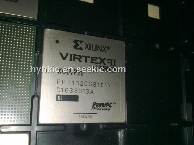
The XC2VP20-6FF1152I is a Platform Flash.
Parametrics
XC2VP20-6FF1152I absolute maximum ratings: (1) Internal supply voltage relative to GND : -0.5 to +4.0V; (2) I/O supply voltage relative to GND : -0.5 to +4.0V; (3) JTAG I/O supply voltage relative to GND : -0.5 to +4.0V; (4) Storage temperature (ambient) : -65 to 150℃; (5) Junction temperature : +125℃.
Features
XC2VP20-6FF1152I features: (1)In-System Programmable PROMs for Configuration of Xilinx FPGAs; (2)Low-Power Advanced CMOS NOR FLASH Process; (3)Endurance of 20,000 Program/Erase Cycles; (4)Operation over Full Industrial Temperature Range (-40 to +85℃); (5)IEEE Standard 1149.1/1532 Boundary-Scan (JTAG) Support for Programming, Prototyping, and Testing; (6)JTAG Command Initiation of Standard FPGA Configuration; (7)Cascadable for Storing Longer or Multiple Bitstreams; (8)Dedicated Boundary-Scan (JTAG) I/O Power Supply(VCCJ); (9)I/O Pins Compatible with Voltage Levels Ranging From 1.5V to 3.3V; (10)Design Support Using the Xilinx Alliance ISE and Foundation ISE Series Software Packages; (11)3.3V supply voltage; (12)Serial FPGA configuration interface (up to 33 MHz); (13)Available in small-footprint VO20 and VOG20 packages.
Diagrams

| Image | Part No | Mfg | Description |  |
Pricing (USD) |
Quantity | ||||||
|---|---|---|---|---|---|---|---|---|---|---|---|---|
 |
 XC2VP20-6FF1152I |
|
IC FPGA VIRTEX-II PRO 1152FFBGA |
Data Sheet |
|
|
||||||
| Image | Part No | Mfg | Description | |
Pricing (USD) |
Quantity | ||||||
|
XC2V1000 |
Other |
|
Data Sheet |
Negotiable |
|
||||||
|
XC2V1000-4BG575I |
|
IC FPGA VIRTEX-II 575PBGA |
Data Sheet |
|
|
||||||
 |
XC2V1000-4BGG575C |
|
IC VIRTEX-II FPGA 1M 575-MBGA |
Data Sheet |
|
|
||||||
|
XC2V1000-4BGG575I |
|
IC FPGA VIRTEX-II 2M 575-MBGA |
Data Sheet |
|
|
||||||
|
XC2V1000-4FF896I |
|
IC FPGA VIRTEX-II 896FCBGA |
Data Sheet |
|
|
||||||
|
XC2V1000-4FFG896C |
|
IC VIRTEX-II FPGA 1M 896-FBGA |
Data Sheet |
|
|
||||||