(China (Mainland))

Product Summary
.1Power Supply
The power supply of both sides, “VSL” and “VSH”, is monitored by an undervoltagelockout block (UVLO) which enables operation of the corresponding side when thesupply voltage reaches the “on” threshold. Afterwards the internal voltage reference andthe biasing circuit are enabled. When the supply voltage (VSL, VSH) drops below the“off” threshold, the circuit is disabled.
2Logic Inputs
The logic inputs InH, InL and SD are fed into Schmitt-Triggers with thresholds compatibleto 3.3V and 5V TTL. When SD is enabled (low), InH and InL are disabled. If InH is high(while InL is low), OutH is enabled and vice versa. However, if both signals are high, theyare internally disabled until one of them gets low again. This is due to the interlockinglogic of the device. See Figure 3 (section 4.7).
3Gate Driver
2ED020I12-FI features two hard-switching gate drivers with N-channel output stagescapable to source 1A and to sink 2A peak current. Both drivers are equipped with active-low-clamping capability. Furthermore, they feature a large ground bounce ruggednessin order to compensate ground bounces caused by a turn-off of the driven IGBT.
4General Purpose
Operational AmplifierThis general purpose operational amplifier can be applied for current measurement ofthe driven low-side IGBT. It is dedicated for fast operation with a gain of at least 3. TheOP is equipped with a -0.1 to 2V input stage and a rail-to-rail output stage which iscapable to drive± 5mA.
5 General Purpose Comparator
The general purpose comparator can be applied for overcurrent detection of the low sideIGBT. A dedicated offset as well as a pull-up and pull-down resistor has been introducedto its inputs for security reasons.
6. Coreless Transformer (CLT)
In order to enable signal transmission across the isolation barrier between low-side andhigh-side driver, a transformer based on CLT-Technology is employed. Signals, that areto be transmitted, are specially encoded by the transmitter and correspondingly restoredby the receiver. In this way EMI due to variations of GNDH (dVGNDH/dt) or the magneticflux density (dΗ/dt) can be suppresed.To compensate the additional propagation delay
Parametrics
? Fully operational to ±1.2 kV
? Power supply operating range from 14 to 18 V
? Gate drive currents of +1 A / –2 A
? Matched propagation delay for both channels
? High dV/dt immunity
? Low power consumption
? General purpose operational amplifier
? General purpose comparatorFeatures
Features
? Floating high side driver
? Undervoltage lockout for both channels
?3.3 V and 5 V TTL compatible inputs
? CMOS Schmitt-triggered inputs with pull-down
? Non-inverting inputs
? Interlocking inputs
? Dedicated shutdown input with pull-up
? RoHS compliant
Diagrams


| Image | Part No | Mfg | Description |  |
Pricing (USD) |
Quantity | ||||||||||||
|---|---|---|---|---|---|---|---|---|---|---|---|---|---|---|---|---|---|---|
 |
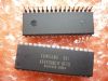
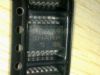
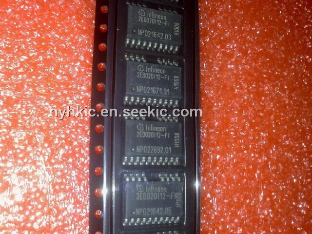
 2ED020I12-FI |
Infineon Technologies |
Power Driver ICs MOS DVR2A Dual Hi/Lo Sde Half Brdg No-Inv |
Data Sheet |
|
|
||||||||||||
| Image | Part No | Mfg | Description | |
Pricing (USD) |
Quantity | ||||||||||||
 |
2ED020I06-FI |
Infineon Technologies |
Power Driver ICs Dual IGBT Driver IC 650V |
Data Sheet |
|
|
||||||||||||
 |
2ED020I12-F |
|
IC DRIVER IGBT 2-CHAN PDSO-18-1 |
Data Sheet |
Negotiable |
|
||||||||||||
|
2ED020I12-FI |
Infineon Technologies |
Power Driver ICs MOS DVR2A Dual Hi/Lo Sde Half Brdg No-Inv |
Data Sheet |
|
|
||||||||||||