(China (Mainland))

Product Summary
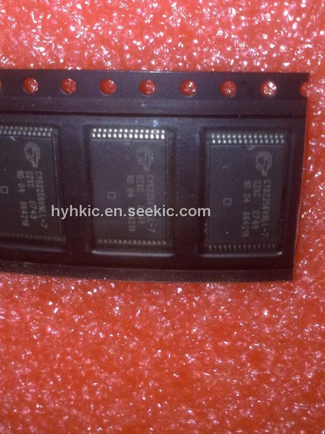
The CY62256VN family is composed of two high-performance
CMOS static RAM’s organized as 32K words by 8 bits. Easy
memory expansion is provided by an active LOW chip enable
(CE) and active LOW output enable (OE) and tri-state drivers.
These devices have an automatic power-down feature,
reducing the power consumption by over 99% when
deselected.
An active LOW write enable signal (WE) controls the
writing/reading operation of the memory. When CE and WE
inputs are both LOW, data on the eight data input/output pins
(I/O0 through I/O7) is written into the memory location
addressed by the address present on the address pins (A0
through A14). Reading the device is accomplished by selecting
the device and enabling the outputs, CE and OE active LOW,
while WE remains inactive or HIGH. Under these conditions,
the contents of the location addressed by the information on
address pins are present on the eight data input/output pins.
The input/output pins remain in a high-impedance state unless
the chip is selected, outputs are enabled, and write enable
(WE) is HIGH.
Features
? Temperature Ranges
— Commercial: 0°C to 70°C
— Industrial: –40°C to 85°C
— Automotive-A: –40°C to 85°C
— Automotive-E: –40°C to 125°C
? Speed: 70 ns
? Low voltage range: 2.7V–3.6V
? Low active power and standby power
? Easy memory expansion with CE and OE features
? TTL-compatible inputs and outputs
? Automatic power-down when deselected
? CMOS for optimum speed/power
? Available in standard Pb-free and non Pb-free 28-lead
(300-mil) narrow SOIC, 28-lead TSOP-I and 28-lead
Reverse TSOP-I packages
Diagrams
| Image | Part No | Mfg | Description |  |
Pricing (USD) |
Quantity | ||||||||||||
|---|---|---|---|---|---|---|---|---|---|---|---|---|---|---|---|---|---|---|
 |
 CY62256VNLL-70ZXC |
Cypress Semiconductor |
SRAM SLo 3.0V ULTRA Lo PWR 32KX8 SRAM |
Data Sheet |
|
|
||||||||||||
|
CY62256VNLL-70ZXCT |
Cypress Semiconductor |
SRAM SLo 3.0V ULTRA Lo PWR 32KX8 SRAM |
Data Sheet |
|
|
||||||||||||